Following is an article noting some aspects of the prototype NBSC Televisor.
Thankyou to all the people on the NBTVA forums, without whose help I would not have been so encouraged to contrinue!
In this article a brief outline will be given of the circuitry developed for an NBSC prototype televisor.
This article is not a general article about televisor building. For details of this please see the NBTVA website and may I recommend the purchase of the Club's handbook in printed form which is a good, clear, simple and cheap way of getting started and always useful for reference. The weblink above has selected chapters of the handbook online too.
The televisor described here is a pretty hastily built Nipkow Disc televisor driven by the motor taken from a popcorn maker. This is controlled by a Club Standard motor control circuit built on stripboard using part robbed from old computer power supplies.
The signal input stage is handled by Klaas Robers' sync seperator circuit which is built on a PCB available from the NBTVA club shop. This is very handy as it gives a fair amount of gain, enough to adjust for most signal sources and outputs a reliable line sync pulse, frame sync pulse and a buffered video output.
In the following sections each component of the colour decoder will be described in turn.
This circuit is presented in the hope that it will be useful as a starting point, stimulate debate, criticism, improvement – it is not expected to be a brilliant example of circuit design and certainly not the best or only way of decoding the signal! However as a prototype it has proved to work reasonably well.
The picture below shows an overview of the colour decoder board.
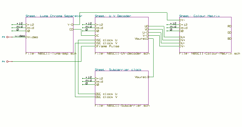
The inputs to the decoder are:
The outputs are positive R, G and B signals at levels of roughly 3V for black and 11V for full modulated (the offset for each channel can be adjusted independently in the matrix). These signals have no gamma correction applied and can be fed direct to most LED drivers (if you require smaller signal swings or to implement a “contrast” control the video input can be attenuated by about 3-4 times and the system works ok, below a certain amount you will need to change the gain of the colour burst amplifier).
In this televisor the R, G, B output are fed to standard single FET Led drivers which provide (rough) gamma correction using a combination of diodes and resistors in the FET source.
Each of the four building blocks at the bottom will be discussed below. The interconnections between them are as follows:
The circuit below shows the luma / chroma seperator.
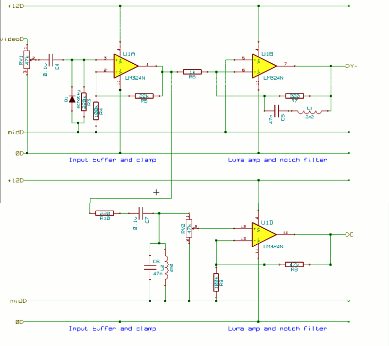
This part of the circuit is fairly simple and is a pair of simple filters to extract the Y and Chroma signals from the combined video input signal. For future improvements more thought will be given to the form of the filters used to better preserve and isolate the two signals: reducing patterning and cross-colour and improving luminance bandwidth. Particularly the choice of inductors was not a good one (the inductors being a little too small for the frequencies but these were the only ones to hand!)
The first op-amp buffers the incoming video - the contrast can be set with the potentiometer -and sets the black level to be just above the “mid” level (with a simple diode clamp - improved clamping could be acheived by using the line-sync pulse and a transistor clamp at this point in the circuit. However for most signals this circuit works satisfactorily.
The top-right op-amp forms a notch-filter which filters out frequencies around 15kHz from the video signal (to reduce dot-structure patterning) and inverts the signal giving the Y- signal.
The bottom op-amp forms a band-pass filter and amplifier which extracts signals centered around 15kHz, the potentiometer can be used to set the colour saturation (colour control).
This is the heart of the decoder, the Chroma signal is demodulated using two double-pole analogue switches to produce the U and V signals (and also inverted versions of U and V needed for the colour matrix)
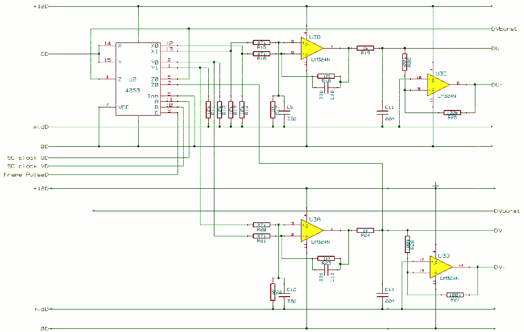
To demodulate the U signal the chroma signal is fed (via the analogue switch 4053) for the first 180 degrees of the in-phase subcarrier (SC clock U) to the non-inverting input of the op-amp and for the remainder to the inverting input. The signal is then low-pass filtered via the resistor capacitor combination (again better filtering could be applied here) before being sent out to the colour matrix. This demodulates the U signal from the QAM colour signal (see here).
[The 4053 analogue switch connects the X input to X1 when A is high and to X0 when A is low, similarly with Y/B and Z/C. It should be noted there are other ways of demodulating a QAM modulated signal but this switching method proved to be very simple to design and in practice works quite well.]
The V signal is demodulated similarly but using the subcarrier signal shifted by 90 degrees (or delayed by 16.6666uS !) (SC clock V).
The 10k resistors at the outputs of the switches pull the outputs to “mid” when the switch is off (otherwise the outputs float and noise can be picked up).
One of the most important aspects of NTSC is that the phase of the local subcarrier oscillator and that at the transmitter must be kept in alsmot perfect synchronisation - 5 degrees of error being about the outer limit before "hue errors" become objectionable. To acheive this a colour burst (a brief burst of unmodulated subcarrier at 0° phase angle) is sent at the start of each frame (in normal NTSC this is sent at the start of each line but the NBTV signal does not allow room for this).
To perform the synchronisation, the V signal is sampled during the frame pulse (via the third analogue switch channel) to produce the Vburst signal. This signal should be "mid" (i.e. 0) for an in sync s/c oscillator any deviation above or below the mid value indicates that the phase is too advanced or retarded. This error signal is fed to the local subcarrier oscillator circuit (next section) and used to adjust the speed of the subcarrier clock. This forms a feedback loop that keeps the local oscillator in sync with the transmitter (hopefully!)
This proved to be the most involved (and frustrating!) part of the circuit to get working. As a crystal oscillator is used it can only be “pulled” a few parts per million in either direction, this means that the source of signals has to be transmitted at a near “perfect pitch”. The author struggled to get this circuit to work until he realised that his £7 crappy CD player was playing back very slow thus the circuit could not achieve “lock”.
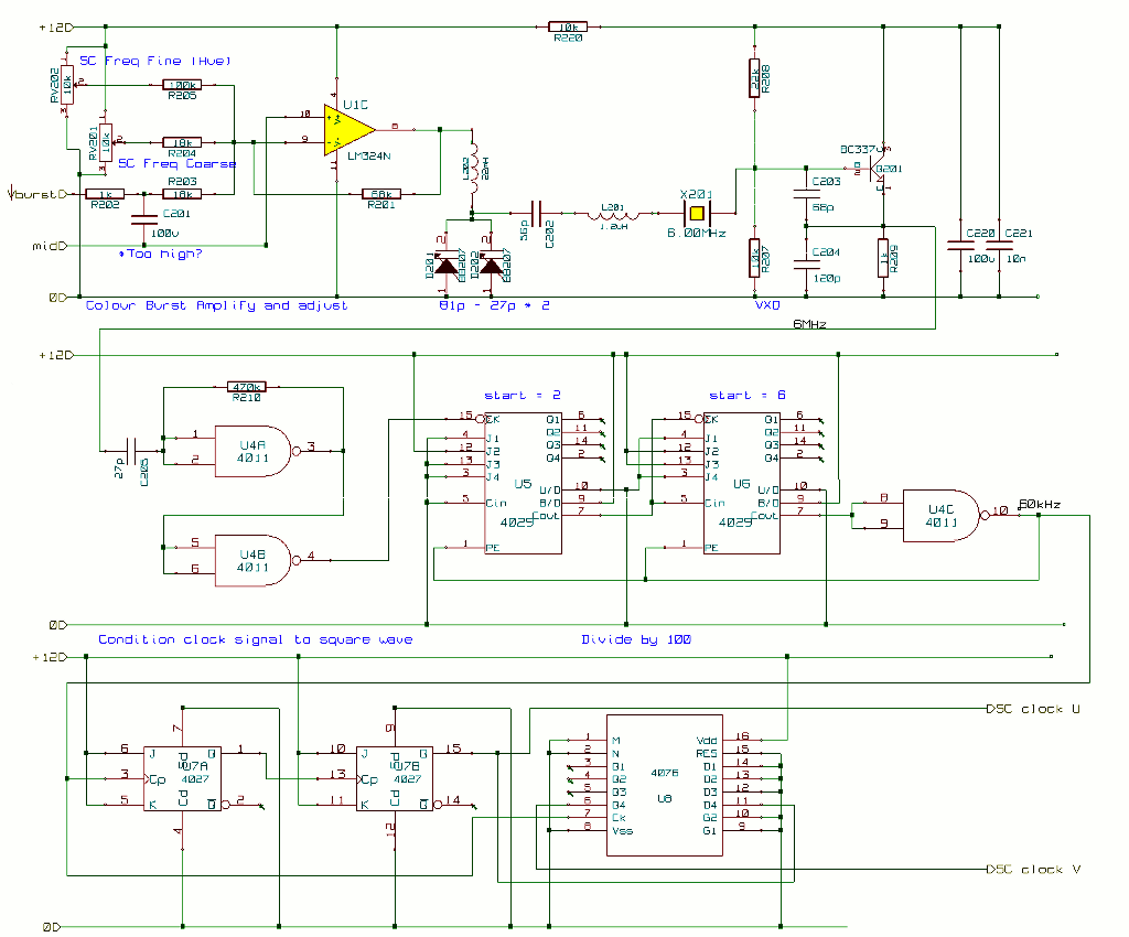
The top-right part of the circuit is a VXO (variable frequency crystal oscillator) running at 6MHz +/- about 140ppm (i.e. +/- 840Hz). The frequency is varied by changing the voltage at the junction of the two varicap diodes. This voltage is the combination of three signals – a coarse setting (which sets the general frequency range of the VXO – a trimmer on the circuit board) – a fine setting (or Hue control) which sets the nominal frequency but a much finer grained user control and the Vburst signal.
If all is running well and the signal source is perfect then the oscillator would be set using the coarse and fine controls to be running at exactly 6MHz. The Oscilaltor would then be sped up or slowed down by the Vburst signal during the colour bursts to bring the generated sub-carrier signals into perfect phase alignment. However the user may intentionally offset the frequency a little using the hue-control and this will mean that to bring the circuit into balance a small phase error must be present on Vburst to achieve a “zero” signal at the output of the Burst amplifier.
The signal is then picked off from the transistor oscillator and passed through two NAND gates to make it into a more perfect square wave. This signal is then passed through a pair of 4-bit clock which divide the frequency by 100 to give a 60kHz signal.
This 60kHz signal is further divided by two twice (using two JK flip-flops configured as T-flip-flops) to produce the in-phase 15kHz square wave. This SC clock U signal is then fed through a D type latch which is clocked by the 60kHz signal, effectively delaying it by 90 degrees to give the SC clock V signal.
A rather tricky aspect of using burst lock that the author did not fully appreciate until recently is the phenomenon of "side-lock". This is an side-effect of using a phase locked loop that is only synchronised periodically. Because we are only receiving a colour burst 12.5 times a second (once every 80ms) we are not receiving a pure sine wave but a sine wave modulated by a square wave of 12.5Hz, this gives many "sidebands" spaced at 12.5Hz either side of required 15kHz if the crystal oscillator is capable of being "pulled" more than 12.5Hz either side of the required 15kHz it is likely that it will lock to one of these side bands instead of the required signal the author can confirm that this does happen and cause much confusion and consternation. Another way of thinking about it is that during the burst - the phase is (on average) correct but during the rest of the frame it goes through a complete (number of) cycle(s) of phase.
The picture above show the effects of "side-lock" the colours cycle throughout the frame. In a moving picture there is also a nausea inducing flicker!
On occasion the televisor gets stuck in sidelock, this necessitates fiddling with the tint control to try and pull the oscillator back into control. It should be possible to fix this by reducing the range of the VXO to a smaller "pull" range (+/- 80ppm) and adjusting the center frequency to be spot on 6MHz. However not having an appreciation of side-lock when designing the VXO the author actually tried to extend the pull range!
A better (cheaper and less complex) solution would be to use a 60kHz watch crystal - these are readily available from suppliers such as Farnell. In early experimentation the author gave up on these as their pull range was far less than normal computer crystals. However the pull range need not be that great (in fact should not be). The initial experiments were abandonded as it was impossible to lock to the cheap (bad) CD players. However the current circuit arrangement has been retained for the prototype, each counter's initial state can be set using switches (U5,6 J1-4) to give different sub-carrier frequencies for further experimentation.
The final stage is to take the Y-, U,U-,V,V- signals and add them together in the correct proportions to give correct red green and blue outputs.
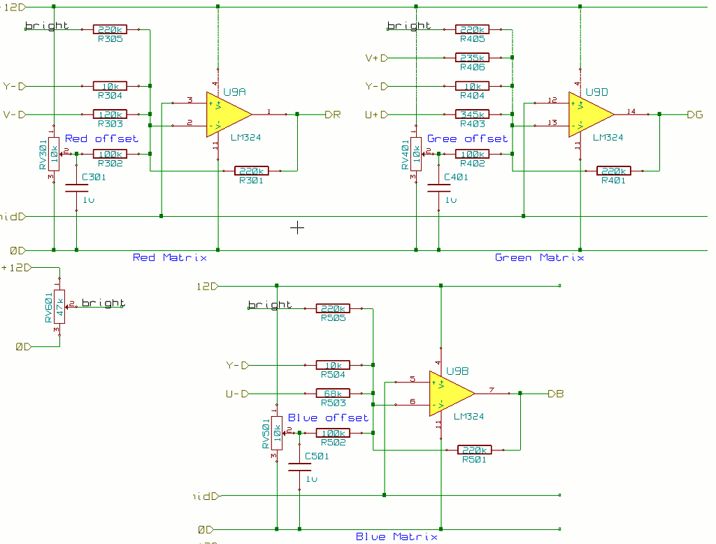
The resistor values used are not “perfect” but were chosen to be close to the correct values whilst using common resistor values (the 345k and 235k resistors can be made up using 330k + 15k, 220k + 15k).
The proportions in which signals are added together are those outlined in the article about NBSC.
A fairly standard circuit arrangment was used to drive each of the LED arrays (one for each primary colour). These circuits need to provide gamma correction. As the brightness increases the diodes in the start to conduct and bypass the source resistor lower resistances giving a rough approximation of the curve required. The actual resistance values in both the source and drain circuits have to be catered for each type of LED - i.e. the red green and blue channels need slightly different values due to the differences in forward voltage drope and current.
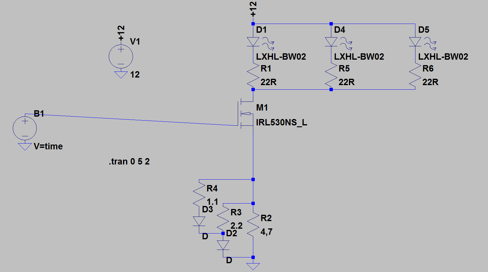
In the actual circuits each channel (red, green, blue) also has a simple gain control comprising a potentiometer at the input, this allows each channel's gain to be set independently to allow correct 9. Test, Alignment and setup.
Using a Nipkow disc we need a light source that will produce a uniformly illuminated rectangle of light some distance behind the Nipkow disc that mixes the three primaries equally over the scanned area.
A first attempt was made using Kingbright Superflux LEDs laid out in a hexagonal pattern with 4 LEDs per primary. This gave a very good but dim picture each LED managing less than 1/4 watt.
A second attempt was made using 1 Watt Luxeons with 4 LEDs per channel. This gave a much nicer brighter picture. However the Luxeon "Stars" were chosen for ease of use - each emitter is attached to its own hexagonal heatsink about 1" in diameter. This meant that the area of the LEDs was far larger than the scanned area. To cater for this a small "light-box" was constructed to focus the light down onto a piece of cardboard at a 45° angle to the "window". The window was then covered in a piece of diffusing plastic - a 2x3" cut out from a box of "nappy wipes".
The LEDs were driven by a circuit similar to the one here. The resistor values have to be adjusted for each channel to cater for the different characteristics of the different coloured LEDs.
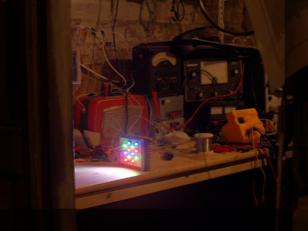
The picture above shows a HDR (high dynamic range) picture of the Luxeon stars mounted to their heatsink. The light output of the stars is quite high - enough to compete with 2 X 100W incandescent light bulbs plus a halogen desk lamp in the small workshop.
The slightly exaggerated image above shows the "purity errors" i.e. the incomplete mixing of the colours at the lightbox output diffuser. In practice this is not quite so pronounced and is barely noticeable when viewing. The imperfections in purity are caused by the fact that "batwing" Luxeons were used (instead of the more preferable Lambertions). These have a sharply illuminated outline to their light profile, which reflects off the insides of the light-box causeing odd "sparkles".
A better choice would be to use a more closely packed group of lambertian Luxeon emitters glued with electrically insulating, heat conducting epoxy direct to the heatsink. This would reduce the need for a complex light box to reduce the area of illumination.
The Televisor was first tested without a sub-carrier oscillator attached to acheive good operation on a regular Black and White signal. The main adjustments similar to a normal televisor were performed i.e.: Front end gain, sync slice level, motor speed, contrast and brightness. The usual messing about getting the motor speed PLL circuit to work and the opto-forks to line up on the disc etc were a little fiddly but nothing out of the ordinary.
Non-standard set up for black and white were the grey-scale tracking controls. This comprises the three controls RV301, 401, 501 on the colour matrix board and the three gain controls at each of the LED drivers. With the contrast and brightness controls set to mid-position. A black and white test card with a set of grey-scale bars was shown and the controls balanced so that each of the grey tones was grey. Any error in the setup of one channel would lead to certain grey tones showing with a hue.
The author fully expected this adjustment to be problematic in that any offset of the background or gain of one channel might upset the gamma curve and produce odd hues. However in practice no problems were experienced, other than the fact that the RV301,401 and 501 controls were given too much gain and so their setting is rather critical.
Next the colour decoder needed to be tested. When the decoder was first built and tested the sub-carrier oscillator had not been built and the circuits could be tested by using a fairly stable RF signal generator to produce a reference sine-wave which was then divided down by a few logic gates to 15kHz. The output of this was plugged into the "SC clock U" and "SC Clock V" lines and an "unlocked" colour picture was received straight away. To acheive "colour lock" with this manual system requred a fair amout of fiddling with the fine tuning control on the sig-gen. However a colour picture was acheived straigh out of the box with no setting up required other than to adjust the saturation control.
Finally the sub-carrier oscillator board was constructed, the final board is slightly different to that published above. The coarse hue control having been removed and replaced by a small "frequency set" trimmer in parallel with the varicap diodes. This is set to acheive reasonable colour lock, the hue control can then be used to fine tune the colours.
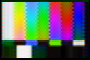
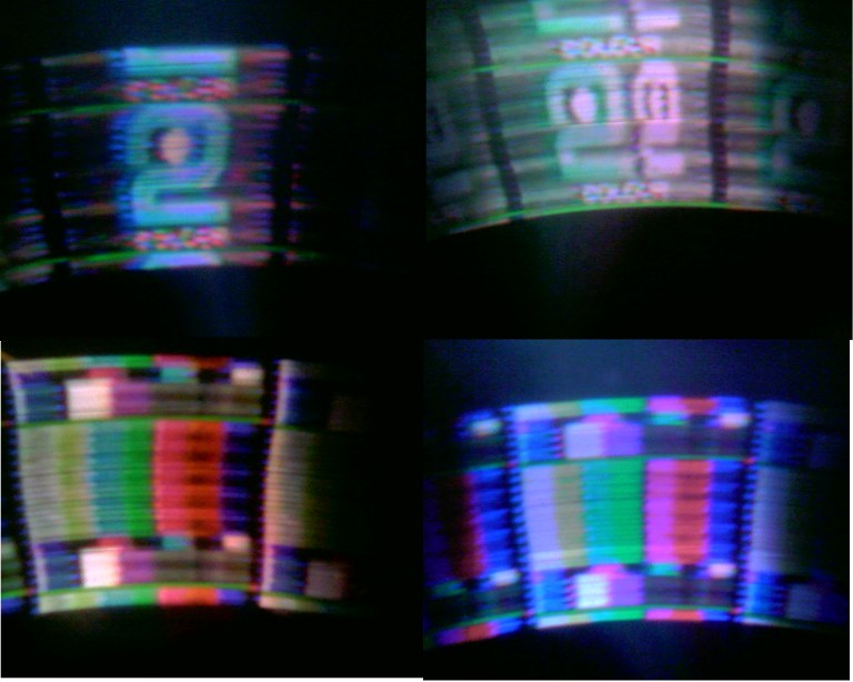
To help with the "hue" setup a back-panel control has been added that grounds the inputs to the red and green LED drivers providing a blue only channel. When this is enabled when viewing an SMPTE colour test card the hue can be set correctly by adjusting the control until every other colour bar shows witht he same intensity. The picture above shows three testcards, the top row how the hue control set too far one way, the middle is correct, the bottom too far the other way. The errors on the test card are just discernible, however when viewing the blue channel only the errors are more apparent and the correct position can be found very quickly.
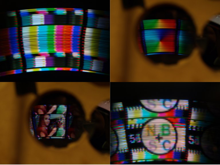
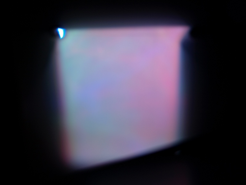
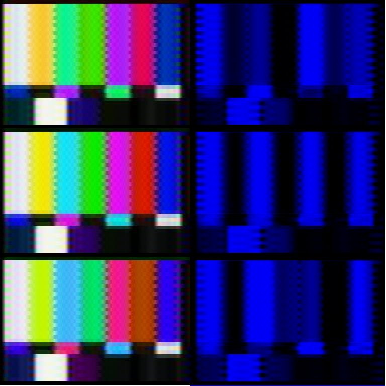
The results of this first experimental televisor are quite encouraging the dot-patterning is not too noticeable and the cross colour even with this very simple circuitry and suck it and see filtering is pretty good. The montage above shows a few screen shots taken from the televisors. More pictures and videos are available in the gallery.
A final proof of the pudding test was to transmit some pictures and pick them up on the televisor. To this end a home built AM-microtransmitter was modified to give the required bandwidth roughly 10Hz to 16kHz at better than 6dB down. For this experiment no particular care was taken with the transmitter other than to ensure a reasonable LF response (to help maintain reasonable sync).
For the receiver I built a quick and dirty dead-bug version of this homodyne receiver (Scroll down to Mar 1972 homodyne). with the filtering arrangments altered to give a wider bandwidth (about 3dB from 10Hz to 22kHz)
The results were very good even on a crowded medium wave band at midnight with lots of interference from ADSL and heterodyne whistles from about 4 different European stations being picked up (the bandwidth of the set is quite wide (about 45kHz) so coveres a few stations!).
The pictures above show a few of the signals radiated from the first floor of the house through about 8" of reinforced concrete and past a lot of noisy equipment to the cellar. A frequency of about 600kHz was chosen as being about the most quite part of the available spectrum in the area (West Yorkshire, UK).
The main problem with reception was to obtain a good clean sync. Due to the NBTVA using "missing" sync for the frame detection any noise can be picked up and detected as a sync and so the frame end is never detected. This leads to difficulty in gettin the disc to spin nicely but also upsets the hue of the picture momentarily as the receiver does not know where to find the colour burst. However once sync was established a good picture could be had with the colour very stable. Some horizontal bar patterning can also be seen - this is due to poor HT regulation in the transmitter letting through mains hum.
 NBSC
NBSC